IBM Packs Nearly 100 Billion Transistors Into a Fingernail-Sized, Sub-1 Nanometer Chip by Stacking Them in Layers

Engineers at IBM crossed a long-standing boundary in semiconductor design this week. They produced working technology for chips with features smaller than one nanometer by arranging transistors in vertical stacks rather than laying everything out on a single flat plane.
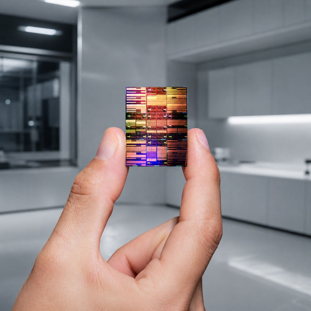
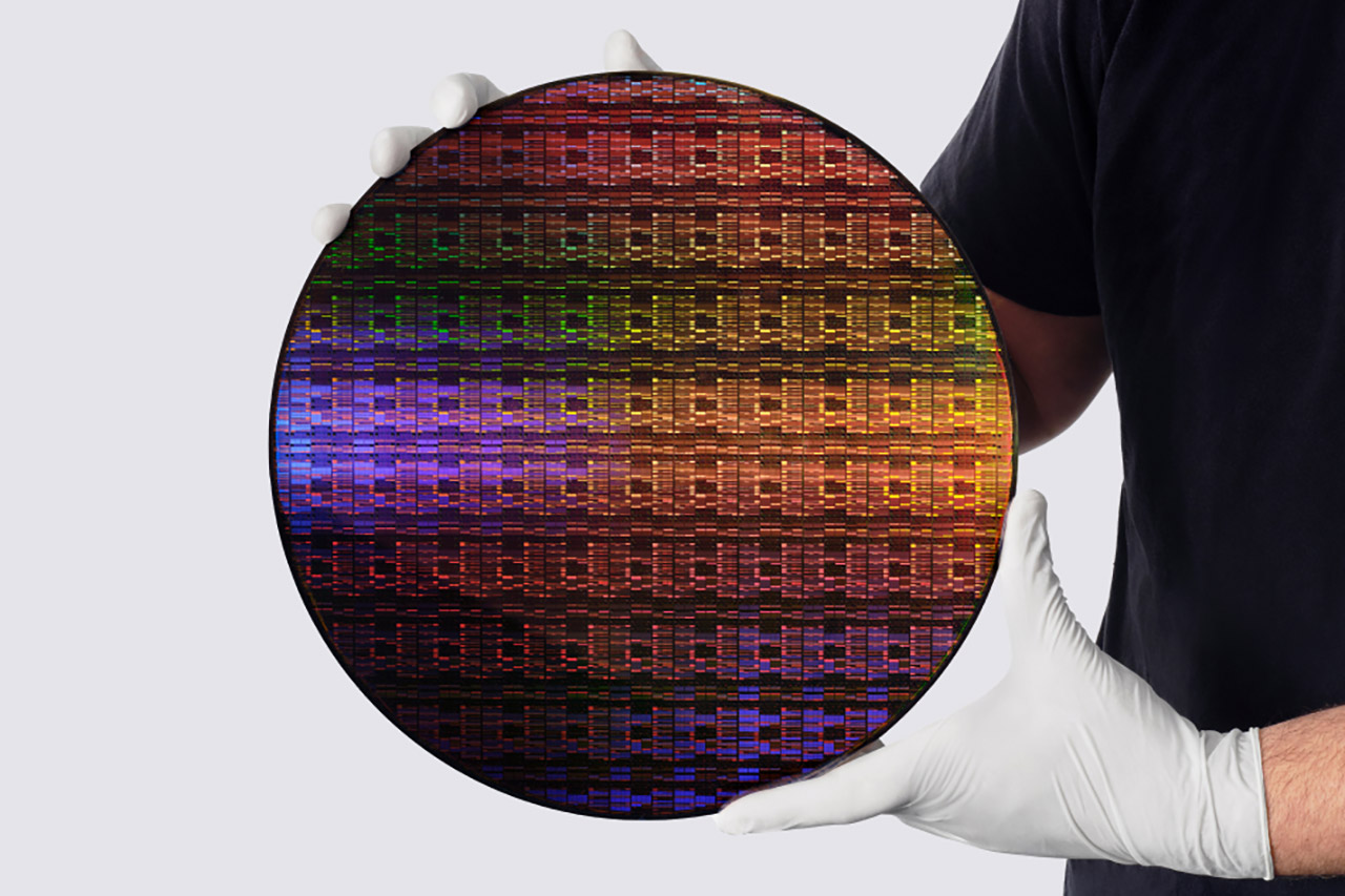
The nanostack technique is the most recent iteration of IBM’s nanosheet transistors, which have been under development for some time. Rather than merely trying to cram more transistors into smaller spaces, the team has decided to take the opposite approach: let’s go higher. They are using the third dimension to fit more transistors on a device. They’re really cramming them in, as a newly completed test chip can fit about 100 billion transistors in a space roughly the size of a fingernail, almost double the density of their 2-nanometer designs from 2021.
Sale

AMD Ryzen 7 7700X 8-Core, 16-Thread Unlocked Desktop Processor
- This dominant gaming processor can deliver fast 100+ FPS performance in the world’s most popular games
- 8 Cores and 16 processing threads, based on AMD “Zen 4” architecture
- 5.4 GHz Max Boost, unlocked for overclocking, 80 MB cache, DDR5-5200 support

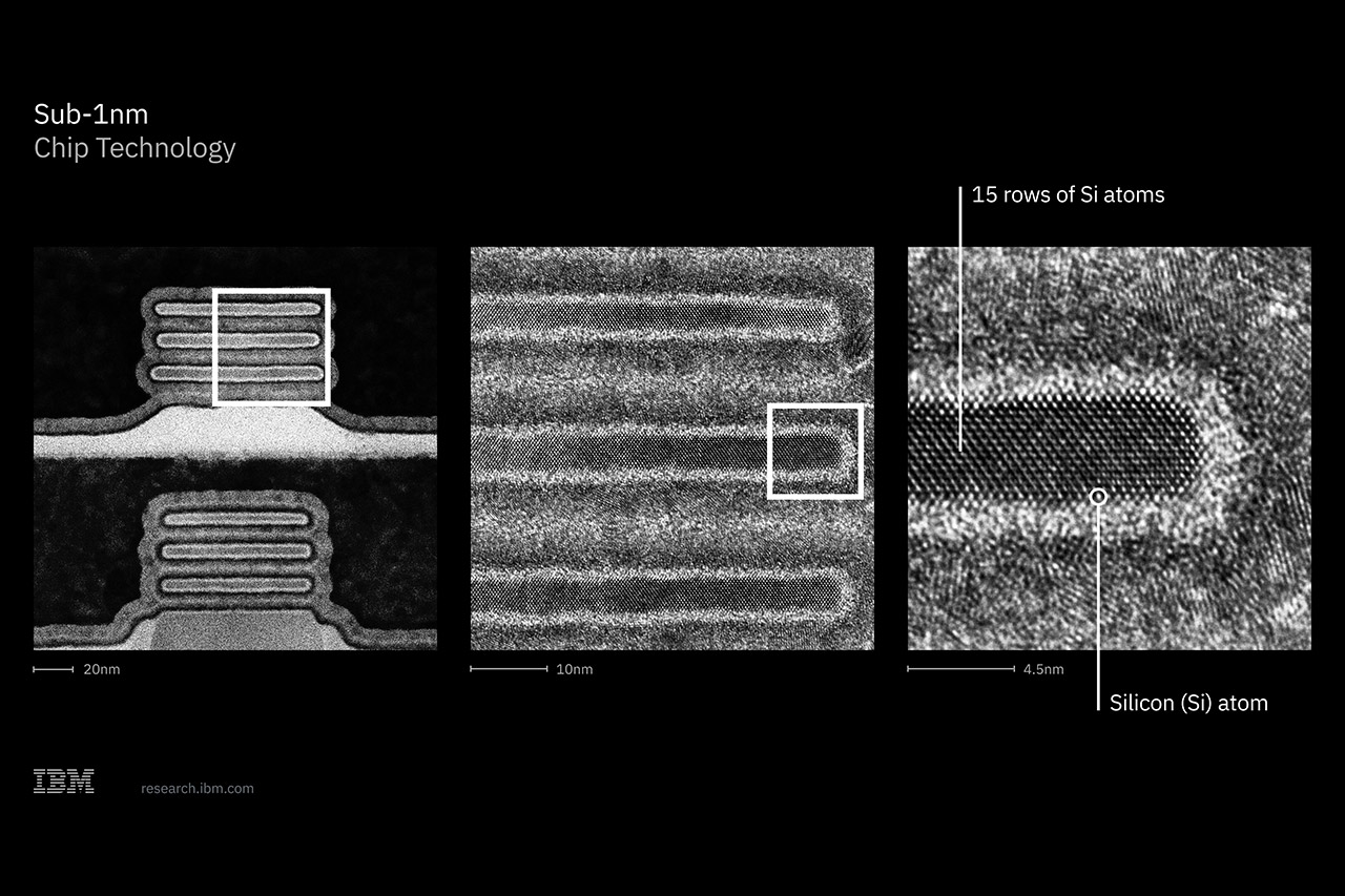
It all depends on a precise technique called wafer bonding, which entails fusing two thin wafers together such that one set of transistors sits precisely on top of another. Because you’re working with atomic scales, this bonding process must be accurate to ensure that the entire thing continues to function as a single unit. Inside each of these stacked transistors, there are three extremely thin silicon nanosheets, each around 5 nanometers thick, that form the real channel through which the current flows. These are small, with fifteen rows of silicon atoms. The thickness of each layer is approximately 9 nm.
They’ve also done some brilliant work with how they lay these out, since the staggered design allows you to fit more transistors in a smaller space while still allowing room for some much-needed wiring and power delivery on the reverse side of the chip. The results are quite impressive: chips made with this new design can run up to 50% quicker or consume up to 70% less energy than the prior 2-nanometer design. Memory blocks also get a boost. SRAM portions, which are essentially the chip’s memory, reduce by 40% in height, which is significant because it means the chip can begin to keep up with all of the advances in how the actual logic stuff works.

They’ve even set up working CMOS inverters and basic circuits to test the concept. The actual hardware development took place at the Albany, NY plant, with assistance from some of the usual suspects, including Lam Research, Tokyo Electron, SCREEN Semiconductor Solutions, and others. And a big thanks to ASML for lending them their extreme ultraviolet lithography tools (those tiny patterns won’t draw themselves). Jay Gambetta, head of IBM Research, described the breakthrough as a watershed moment that will radically alter the way we think about computing and how we design devices that can stay up.
[Source]
IBM Packs Nearly 100 Billion Transistors Into a Fingernail-Sized, Sub-1 Nanometer Chip by Stacking Them in Layers
#IBM #Packs #Billion #Transistors #FingernailSized #Sub1 #Nanometer #Chip #Stacking #Layers